Building systems with SERV
A CPU is only as good as its ecosystem. In order to make use of SERV, it needs to be combined with other components such as memories, accelerators and peripheral controllers.
Welcome to the reservoir, a pool of ready-made designs and subsystems for different purposes that you can use to quickly get started with SERV or integrate it into larger designs.
Servile : Convenience wrapper
Servile convenience wrapper
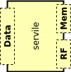
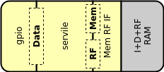
Servile is a helper component that takes care of common configuration and is used as a building block in the other designs and subsystems. It exposes a memory bus intended to be connected to a combined data and instruction memory, an extension bus for peripheral controllers and accelerators and an RF interface for connecting to an SRAM for GPR and CSR registers.
Servile block diagram
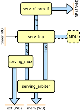
Internally, Servile contains logic for optionally instantiating an MDU core for the M extension, an arbiter to route instruction fetches and main memory accesses through the same interface and a mux to split up the memory map into memory (0x00000000-0x3FFFFFFF) and external accesses (0x40000000-0xFFFFFFFF). The mux also contains simulation-only logic to write output to a log file and stop the simulation.
Parameters
Parameter |
Values |
Description |
|---|---|---|
reset_pc |
0x00000000 (default) - 0xFFFFFFFC |
Address of first instruction to fetch from memory after reset (Reset vector) |
reset_strategy |
“MINI” (default), “NONE” |
Amount of reset applied to design
“NONE” : No reset at all. Relies on a POR to set correct initialization values and that core isn’t reset during runtime
“MINI” : Standard setting. Resets the minimal amount of FFs needed to restart execution from the instruction at RESET_PC.
|
rf_width |
2 (default), 4, 8, 16, 32 |
Width of the data bus to the RF memory. Typically smaller values use less resources, but can be implementation-dependant. |
sim |
0 (default), 1 |
Enable simulation mode. In simulation mode, two memory addresses have special purposes.
0x80000000: Writes to this address puts the byte in the lowest data byte into a log file decided by the “signature” plusarg.
0x90000000: Writes to this address ends the simulation.
|
with_c |
0 (default), 1 |
Enable the C extension. This also makes SERV support misaligned loads and stores. |
with_csr |
0 (default), 1 |
Enable the Zicsr extension. This also enables timer IRQ and exception handling. Note that SERV only implements a small subset of the CSR registers. |
with_mdu |
0 (default), 1 |
Enables the Multiplication and Division Unit (MDU) to support the M extension. Note that this only enables the interface and the decoder logic. The MDU itself is external from SERV. |
Signals
Signal |
Width |
Direction |
Description |
|---|---|---|---|
i_clk |
1 |
in |
Clock |
i_rst |
1 |
in |
Synchronous reset |
i_timer_irq |
1 |
in |
Timer interrupt |
Memory interface |
Connect to instruction/data memory |
||
o_wb_mem_adr |
32 |
out |
Memory bus address |
o_wb_mem_dat |
32 |
out |
Memory bus data |
o_wb_mem_sel |
4 |
out |
Memory bus write data byte select mask |
o_wb_mem_we |
1 |
out |
Memory bus write transaction |
o_wb_mem_stb |
1 |
out |
Memory bus active strobe |
i_wb_mem_rdt |
32 |
in |
Memory bus read data |
i_wb_mem_ack |
1 |
in |
Memory bus cycle acknowledged |
Extension interface |
Connect to peripheral controllers |
||
o_wb_ext_adr |
32 |
out |
Data bus address |
o_wb_ext_dat |
32 |
out |
Data bus write data |
o_wb_ext_sel |
4 |
out |
Data bus write data byte select mask |
o_wb_ext_we |
1 |
out |
Data bus write transaction |
o_wb_ext_stb |
1 |
out |
Data bus active cycle |
i_wb_ext_rdt |
32 |
in |
Data bus return data |
i_wb_ext_ack |
1 |
in |
Data bus return data valid |
RF (SRAM) interface |
|||
o_rf_waddr |
ceil(log2(regs*32/rf_width) |
out |
RF memory write address |
o_rf_wdata |
rf_width |
out |
RF memory write data |
o_rf_wen |
1 |
out |
RF memory write enable |
o_rf_raddr |
ceil(log2(regs*32/rf_width) |
out |
RF memory read address |
i_rf_rdata |
rf_width |
out |
RF memory read data |
o_rf_ren |
1 |
out |
RF memory read enable |
Serving : FPGA subsystem
Serving SoClet
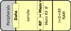
Serving is ideal for FPGA implementations as it only uses a single combined block RAM for instructions, data and RF that can be preloaded with a RISC-V application. It exposes a wishbone data bus that can be used to connect peripheral controllers.
Parameters
Parameter |
Values |
Description |
|---|---|---|
memfile |
“” (default) |
Verilog hex file containing a RISC-V application to be preloaded into memory |
memsize |
1-4294967296 (default 8192) |
Size of memory (in bytes). Needs to be at least large enough to fit the application supplied by memsize. Note that the RF occupies the highest 128 bytes of memory in the RAM. |
sim |
0 (default), 1 |
Enable simulation mode. In simulation mode, two memory addresses have special purposes.
0x80000000: Writes to this address puts the byte in the lowest data byte into a log file decided by the “signature” plusarg.
0x90000000: Writes to this address ends the simulation.
|
RESET_STRATEGY |
“MINI” (default), “NONE” |
Amount of reset applied to design
“NONE” : No reset at all. Relies on a POR to set correct initialization values and that core isn’t reset during runtime
“MINI” : Standard setting. Resets the minimal amount of FFs needed to restart execution from the instruction at RESET_PC.
|
WITH_CSR |
0 (default), 1 |
Enable the Zicsr extension. This also enables timer IRQ and exception handling. Note that SERV only implements a small subset of the CSR registers. |
Signals
Signal |
Width |
Direction |
Description |
|---|---|---|---|
i_clk |
1 |
in |
Clock |
i_rst |
1 |
in |
Synchronous reset |
i_timer_irq |
1 |
in |
Timer interrupt |
Extension interface |
Connect to peripheral controllers |
||
o_wb_adr |
32 |
out |
Data bus address |
o_wb_dat |
32 |
out |
Data bus write data |
o_wb_sel |
4 |
out |
Data bus write data byte select mask |
o_wb_we |
1 |
out |
Data bus write transaction |
o_wb_cyc |
1 |
out |
Data bus active cycle |
i_wb_rdt |
32 |
in |
Data bus return data |
i_wb_ack |
1 |
in |
Data bus return data valid |
Servant : FPGA Reference platform
Servant FPGA Reference platform
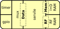
SERV comes with a small FPGA-focused reference platform called Servant, which is capable of running Zephyr RTOS, the regression test suite and other software. The platform consists of SERV, a timer, memory and a 1-bit GPIO output pin.
Available targets
The servant SoC has been ported to an increasing number of different FPGA boards and is easy to modify for new targets. To see all currently supported targets run:
fusesoc core show servant
By default, these targets have the program memory preloaded with a small Zephyr hello world example that writes its output on a UART pin. Don’t forget to install the appropriate toolchain (e.g. icestorm, Vivado, Quartus…) and add to your PATH
Some targets also depend on functionality in the FuseSoC base library (fusesoc-cores). Running fusesoc library list should tell you if fusesoc-cores is already available. If not, add it to your workspace with
fusesoc library add fusesoc-cores https://github.com/fusesoc/fusesoc-cores
Now we’re ready to build. Note, for all the cases below, it’s possible to run with –memfile=$SERV/sw/blinky.hex (or any other suitable program) as the last argument to preload the LED blink example instead of hello world.
AC701
fusesoc run –target=ac701 servant
Alchistry AU
fusesoc run –target=alchistry_au servant
Alhambra II
Pin 61 is used for UART output with 115200 baud rate. This pin is connected to a FT2232H chip in board, that manages the communications between the FPGA and the computer.
fusesoc run –target=alhambra servant iceprog -d i:0x0403:0x6010:0 build/servant_1.0.1/alhambra-icestorm/servant_1.0.1.bin
Alinx ax309 (Spartan6 LX9)
Pin D12 (the on-board RS232 TX pin) is used for UART output with 115200 baud rate and wired to Pin P4 (LED0).
fusesoc run –target=ax309 servant
Arty A7 35T
Pin D10 (uart_rxd_out) is used for UART output with 57600 baud rate (to use blinky.hex change D10 to H5 (led[4]) in data/arty_a7_35t.xdc).
fusesoc run –target=arty_a7_35t servant
Arty S7 50T
Pin R12 (uart_rxd_out) is used for UART output with 57600 baud rate (to use blinky.hex change R12 to E18 (led[4]) in data/arty_s7_50t.xdc).
fusesoc run –target=arty_s7_50t servant
Chameleon96 (Arrow 96 CV SoC Board)
FPGA Pin W14 (1V8, pin 5 low speed connector) is used for UART Tx output with 115200 baud rate. No reset key. Yellow Wifi led is q output.
fusesoc run –target=chameleon96 servant
CMOD A7 35t
FPGA Pin J18 is used for UART output with 57600 baud rate. btn0 is used for reset.
fusesoc run –target=cmod_a7_35t servant
CYC1000
fusesoc run –target=cyc1000 servant
DE0 Nano
FPGA Pin D11 (Connector JP1, pin 38) is used for UART output with 57600 baud rate. DE0 Nano needs an external 3.3V UART to connect to this pin
fusesoc run –target=de0_nano servant
DE10 Nano
FPGA Pin Y15 (Connector JP7, pin 1) is used for UART output with 57600 baud rate. DE10 Nano needs an external 3.3V UART to connect to this pin
fusesoc run –target=de10_nano servant
DE1 SoC revF
FPGA PIN_AC18 (Connector GPIO0, pin 0) is used for UART output with 57600 baud rate. DE1 SoC revF needs an external 3.3V UART to connect to this pin. The UART pin has not been tested.
fusesoc run –target=de1_soc_revF servant
DECA development kit
FPGA Pin W18 (Pin 3 P8 connector) is used for UART output with 57600 baud rate. Key 0 is reset and Led 0 q output.
fusesoc run –target=deca servant
EBAZ4205 ‘Development’ Board
Pin B20 is used for UART output with 57600 baud rate. To use blinky.hex change B20 to W14 (red led) in data/ebaz4205.xdc file).
fusesoc run –target=ebaz4205 servant
fusesoc run –target=ebaz4205 servant –memfile=$SERV/sw/blinky.hex
Reference: https://github.com/fusesoc/blinky#ebaz4205-development-board
ECP5 EVN
fusesoc run –target=ecp5_evn servant
Icebreaker
Pin 9 is used for UART output with 57600 baud rate.
fusesoc run –target=icebreaker servant
iCEstick
Pin 95 is used as the GPIO output which is connected to the board’s green LED. Due to this board’s limited Embedded BRAM, programs with a maximum of 7168 bytes can be loaded. The default program for this board is blinky.hex.
fusesoc run –target=icestick servant iceprog build/servant_1.4.0/icestick-icestorm/servant_1.4.0.bin
iCESugar
Pin 6 is used for UART output with 115200 baud rate. Thanks to the onboard debugger, you can just connect the USB Type-C connector to the PC, and a serial console will show up.
fusesoc run –target=icesugar servant
iCESugar-nano
Pin B3 is used for LED output. As the default clock of 12 MHz is rather slow the LED only toggles every 9 seconds with the default blinky example.
Thanks to the onboard debugger, you can just connect the USB Type-C connector to the PC, and a serial console will show up. However, the device doesn’t have enough RAM to run the Zephyr hello-world example so the UART pins are not connect but they are defined in the PCF for easy reference.
fusesoc run –target=icesugar-nano servant
ICE-V Wireless
Pin 9 is used for UART output with 57600 baud rate.
fusesoc run –target=icev_wireless servant
iceprog build/servant_1.4.0/icestick-icestorm/servant_1.4.0.bin
GMM7550
fusesoc run –target=gmm7550 servant
LX9 Microboard
fusesoc run –target=lx9_microboard servant
Machdyne Kolibri
Pin B1 is used for UART output with 115200 baud rate. The serial port on Kolibri is accessible as a USB-CDC device.
fusesoc run –target=machdyne_kolibri servant
ldprog -Ks build/servant_1.4.0/machdyne_kolibri-icestorm/servant_1.4.0.bin
MAX10 10M08 Evaluation Kit
FPGA Pin 75 (Arduino_IO01 J5 pin 7) is used for UART output with 57600 baud rate. SW1 is reset and Led 1 q output.
fusesoc run –target=max10_10m08evk servant
Nandland Go Board
Pin 56 is used as the GPIO output which is connected to the board’s LED1. Due to this board’s limited Embedded BRAM, programs with a maximum of 7168 bytes can be loaded. The default program for this board is blinky.hex.
fusesoc run –target=go_board servant iceprog build/servant_1.4.0/go_board-icestorm/servant_1.4.0.bin
Nexys 2
Pmod pin JA1 is connected to UART tx with 57600 baud rate. A USB to TTL connector is used to display to hello world message on the serial monitor. (To use blinky.hex change L15 to J14 (led[0]) in data/nexys_2.ucf).
fusesoc run –target=nexys_2_500 servant –uart_baudrate=57600 –firmware=$SERV/sw/zephyr_hello.hex
Nexys A7
fusesoc run –target=nexys_a7 servant
OrangeCrab R0.2
Pin D1 is used for UART output with 115200 baud rate.
fusesoc run –target=orangecrab_r0.2 servant dfu-util -d 1209:5af0 -D build/servant_1.4.0/orangecrab_r0.2-trellis/servant_1.4.0.bit
PolarFire Splash Kit
Pin R5 is used for UART output with a 115200 baud rate, this is routed through the onboard FTDI transceiver. LED1 (Pin P7) serves as the generic GPIO.
Pin P8 is used as the GPIO heartbeat with a 1Hz frequency and is connected to the board’s LED2.
Pin N4 (user reset) is used for the reset
fusesoc run –target=polarfire_splashkit servant –memfile=$SERV/sw/zephyr_hello.hex
Saanlima Pipistrello (Spartan6 LX45)
Pin A10 (usb_data<1>) is used for UART output with 57600 baud rate (to use blinky.hex change A10 to V16 (led[0]) in data/pipistrello.ucf).
fusesoc run –target=pipistrello servant
SoCKit development kit
FPGA Pin F14 (HSTC GPIO addon connector J2, pin 2) is used for UART output with 57600 baud rate.
fusesoc run –target=sockit servant
Trenz Electronic TE0802
PMOD A marked J5, pin two, on the board is used for UART output with 115200 baud rate.
fusesoc run –target=te0802 servant
TinyFPGA BX
Pin A6 is used for UART output with 115200 baud rate.
fusesoc run –target=tinyfpga_bx servant tinyprog –program build/servant_1.0.1/tinyfpga_bx-icestorm/servant_1.0.1.bin
ULX3S
fusesoc run –target=ulx3s servant
Upduino2
fusesoc run –target=upduino2 servant
zcu106
fusesoc run –target=zcu106 servant
Porting Servant to a new target
Mostly any FPGA board can be used to run the Servant SoC. In its simplest form it just needs an FPGA with a clock input and an output that can be used to connect an UART or a LED.
The porting process consists of FIXME steps. We will use <name> as a placeholder for the name of the FPGA board. 1. Locate the pins used for clock input and for the outputs. Outputs should preferably be both a LED and an UART, but either works if not both are available. Optionally, locate an input pin connected to the reset as well. This is not required, but can be handy. 2. Write a pin constraints file with your located pins in the format of the FPGA toolchain you intend to use. For Vivado this would be an .xdc file. For Quartus a .tcl file, for nextpnr a .pcf file and so on. Save this as data/<name>.{pcf,ucf,xdc…} in the SERV repo. 3. Create a clock generation file 4. Create a top-level 5. Create a fileset 6. Create a target
Subservient : SERV ASIC macro
Subservient ASIC macro
Subservient is a minimal reference system that just requires connecting one single-port SRAM for data, instructions and RF. It is intended to make ASIC integration easier.